What Does a 30-Year Career in Semiconductors Look Like?

Read on the ON Semiconductor blog
by George Chang, Sr. Director of Corporate Program Management, Global Program Management and Manufacturing Engineering
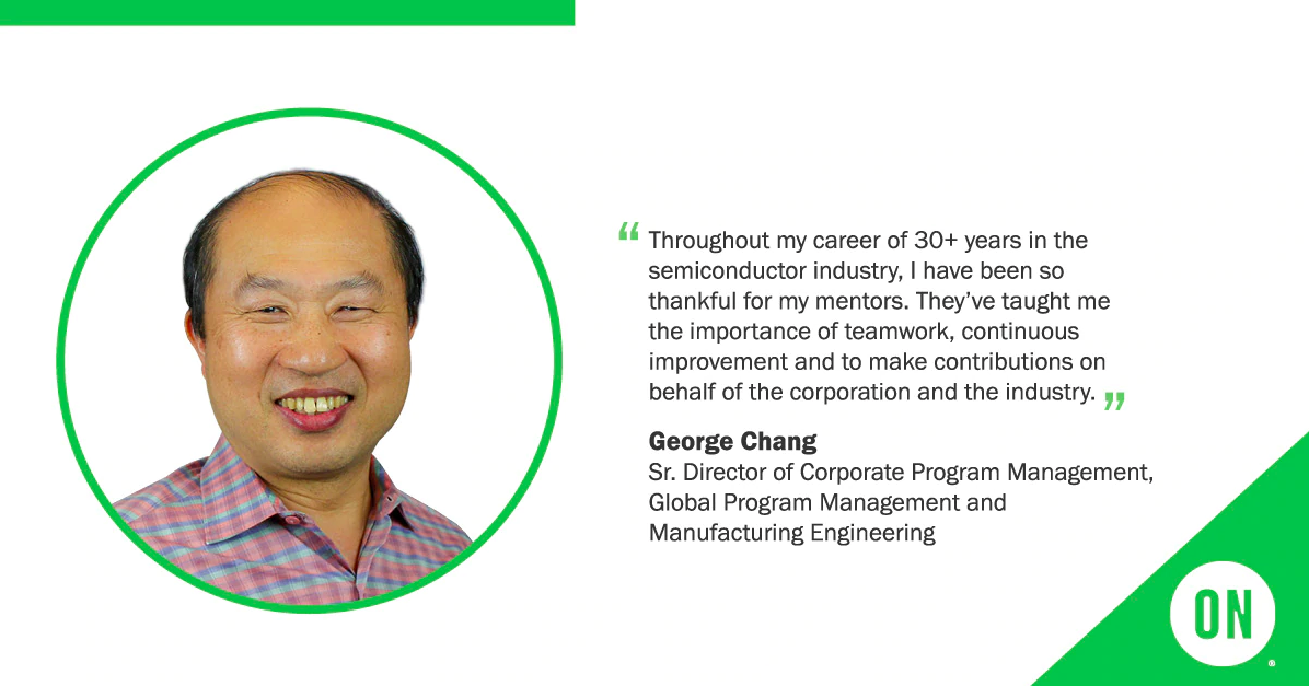
Throughout my career of 30+ years, I have been so thankful for my mentors at the start of my career. They taught me the importance of teamwork and continuous improvement and to make contributions to the corporation and the industry. The engineers from Motorola Aizu, where I started my career, have established my foundation and knowledge within semiconductor operations thirty years ago. Throughout the years, these same mentors have continued to offer encouragement, advocated for personal growth and helped me improve and grow my skill set. I owe many of my accomplishments to them and their persistent guidance. When they first hired me, I didn’t know the industry nor did I understand the language, but look at me now, thirty years into my career and with many achievements, thanks to those who originally believed in me and pushed me to think and innovate.
My parents always wanted me to become a medical doctor. However, I realized that I wouldn’t be able to survive in the medical field after my first biology course. Rather, I enjoyed solving mathematical equations and physics problems, so I decided to study engineering. I studied mechanical engineering in college and focused on the design and material science after my summer internship as a Computer-aided design (CAD) technician. For graduate school, I studied ceramic material’s mechanical properties. When I completed graduate school, I was offered a job at Nippon Motorola Aizu’s plant in Japan (located in the Tohoku region), even though I didn’t have a semiconductor background. Hiring managers focused on one’s potential and believed in on the job training. I convinced recruiters that I was able to quickly learn and adapt. After I joined the Aizu plant, I gave my first Japanese presentation in six weeks and my first Japanese report three months later I decided that I needed to master the Japanese language to perform well in a Japanese company and working environment. I applied the same spirit for my learning of the local language to my learning of semiconductor devices and operations. However, without my co-workers’ instruction and assistance, I would not have been able to learn so quickly. This integration established lifelong friendships. When I return to Aizu, my friends are always waiting for me at the station, to this day.
During my first interview with Nippon Motorola, I told interviewers that I wanted to work on technology transfers and act as the bridge between the technology development department and manufacturing operations. Little did I know then that my entire career would be spent working on technology/new product development, technology transfer within the same original manufacturing company. The first product I managed, was Smart MOSJ (Japanese version Smart Power IC) technology which enabled SONY’s Discman function. Some of the technology I’ve co-developed, like HD plus and HD3e, are still in production after twenty years of production. Through technology transfers, I’ve helped our corporation capture more business, increase revenue and have been a driving force for innovation.
Eventually, I was given an opportunity to manage a fab startup program and was part of the factory staff to implement operational best practices at COM1, a small factory focused on research and development, which was very unique during ON Semiconductor’s first phase of technology manufacturing. I worked with every COM1 member from the re-start of the fab to its eventual closure. During this experience, I gained invaluable insight and experience which has helped me push forward in my career endeavors of continuous improvement. Aside from the many technological developments and a significant amount of shipments from a small fab, the most important outcome has been the lifelong friendships I’ve developed. During startup, every engineer worked twelve hours shifts and broke the boundary of engineer expertise to work on everything we could, which lead to our collaborative team culture. When we were told the news of our factory closure, many of us kept in contact by starting a semi-annual night golf tradition and continued gathering for lunch at Haji Baba. We created a lot of good memories together.
Upon the closure of COM1, one of the largest endeavors I worked on as the corporate device manager for legacy technologies was the Cu wire implementation program, which was significantly cheaper in comparison to Au wire. This allowed me to be the bridge between the fab and the assembly operations with the ability to implement a win-win solution for Cu-wiring. In order to tap into the cost savings from Cu wire, a PAD metal module integration needed optimization to accommodate Cu wire’s material characteristic. Wire bond equipment and process were also necessary adjustments that we needed to make.
In 2011, I was given the opportunity to lead the Sanyo integration on the operations side due to my technical experience and Japanese, I was part of the team to evaluate Sanyo Semiconductor, and worked on acquisition and integration plan. After the acquisition, I was responsible for Sanyo Integration on the operation side. During this integration, I worked on technology transfer and factory consolidation as well as site selection, new site establishment and technology/tool sales. Most importantly, I learned how to integrate and transform our entire operations team to adopt a global business model. Aizu’s joint ventures expanded my operations experience to 8in wafer fab. Together with my friends from Aizu and Gresham/Fujitsu members, we set a new record of technology transfer schedules with multiple transfers working in parallel. In 2019, I was given a chance to expand my experience into 12in wafer operations and technology transfer. Once again, we demonstrated on-time T6 transfer/development into a factory without any discrete operation experience. Our two companies worked extremely well together and were quite successful.
Though Motorola no longer exists, I am incredibly thankful for the opportunity to have launched my career there and to have been adopted into the ON Semiconductor team when they spun off from Motorola in 1999. ON Semiconductor has provided me with an incredible work environment, the ability to work on various projects, with good mentors and co-workers who’ve turned into lifelong friends, and helped me grow and develop both professionally and personally. I must give a shout out to the Nippon Motorola leaders who believed in me thirty years ago to work in a brand new field and in a market where I did not know the local dialect. I told many people that ON Semiconductor was my playground. Work was more than just a place that I showed up to every weekday, it has become a place of intellectual discussions ranging from fundamental theory to academic program management practice, to mental and spiritual encouragement. This has grown and stretched me as a person and is something that I highly value. I’m particularly thankful that I could work on challenging and meaningful programs for our corporation and to collaborate and co-develop several technologies (some of which are still running after twenty years like HD+, HD3e, Trench 1). I’ve invented and applied for 10+ patents and have published quite a few papers over my 30+ year career.
Life is filled with excitement and opportunities. We each need to continue doing our best and show up with a “can-do” attitude. When you start your day think to yourself, “I would like to try with my best effort.” That’s all we can expect from one another.
Consider starting your career journey with us by checking out our open positions today!

